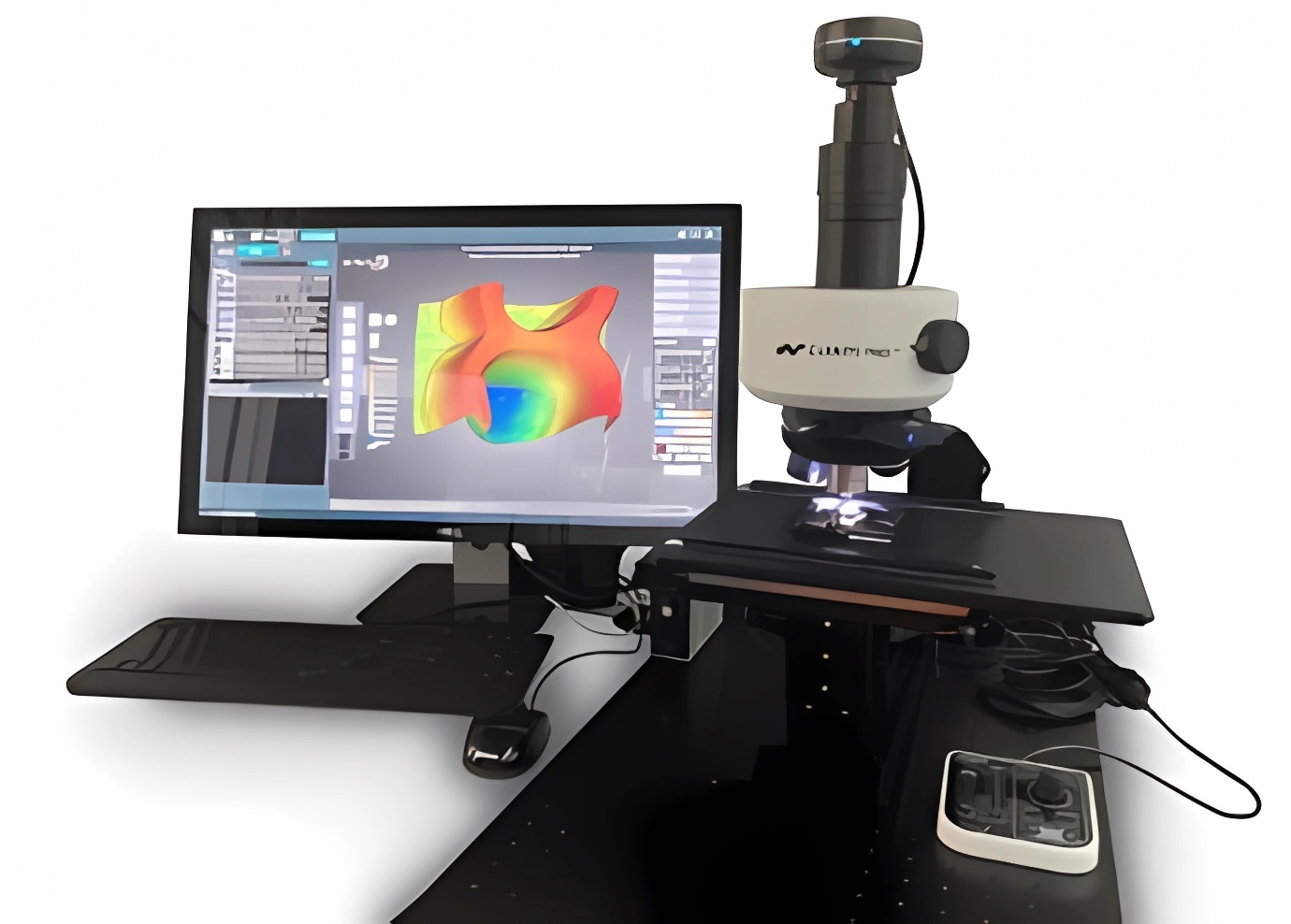
for wafers up to 300mm
Surface analysis and defect review tool that has the combined capabilities of a scanning electron microscope (SEM) and an atomic force microscope (AFM) in one tool. ~1 angstrom z-height detection capability to quickly characterize any surface in 3D in a matter of minutes using Photometric Stereo Technology (PST). User-focused software interface is the easiest to use of any system in the marketplace.
Features
- Patented angstrom-level surface imaging & characterization sequal or better in performance to AFM or SEM
- Proprietary 2D/3D Machine Vision Algorithms and Machine Learning
- Full Wafer Image to Microscope Image With High Magnification Objectives
- Up to 300mm x 300mm substrates w/scanning capability
- Imaging in all optical modalities including BF, DF, DIC, POL & FL
- Available in Manual, Scanning * Modular configurations
- Resolution
- Z-height Resolution ~ 1 angstrom
- X-Y Resolution ~ 200nm for 100X objective (objective dependent)
- Embedded, proprietary AI engine to train defect libraries for classification and follow-on measurements
- KLARF file input for defect review

