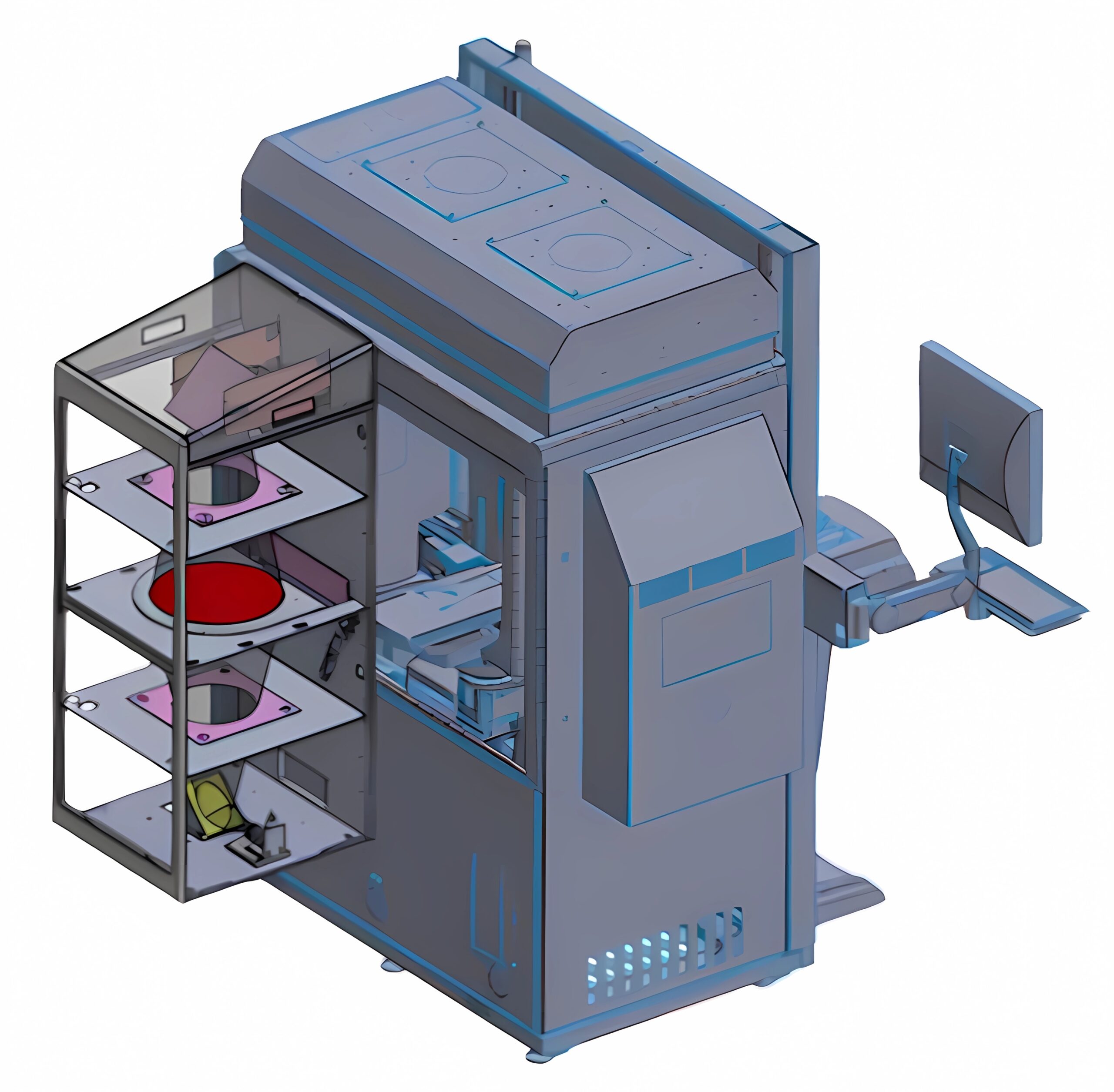
for wafers up to 300mm
Utilizes a proprietary infrared detection scheme, coupled with the powerful Clarity software platform, to quickly characterize bonded wafers for voids, cracks, and delamination, as well as crystal defects in various types of substrates including, GaN, SiC, and diamond. Detects and locates defects and anomalies down to below 1 micron, and the user-focused, easy-to-use software interface quickly classifies them for further process assessment and optimization.
Features
- Patented system design
- Open platform to accommodate large range of sample sizes
- 25mm to 300mm
- BTBP Clarity Software for turnkey solution measurements to SEMI standards
- Resolution
- Sub-micron for Voids & Strain Fields
- Substrate scanned with 17-bit depth in transmission scatter mode (one part in 130,000)
- 100um pixel resolution
- Automation customized for throughput and sample size
- Standalone or automated
- Bolts configuration to SEMI standards for attachment to any EFEM or process tool
- Full wafer scan with 2 to 3mm edge exclusion.
- AI engine to train your own library of defects for classification and measurements
- KLARF file location capability to review
- Turnkey recipe setup software for automation to run batches

