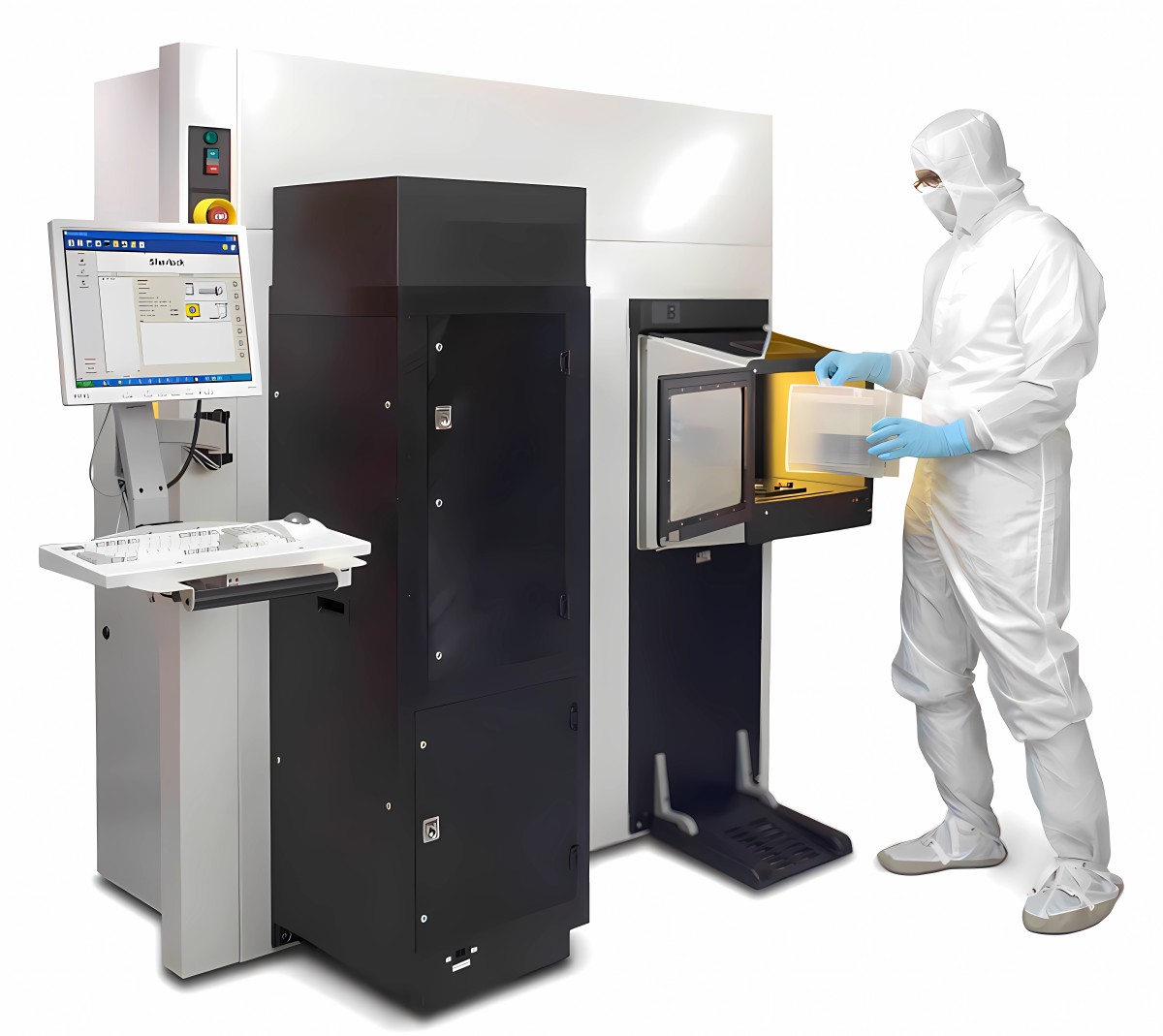
for 100mm to 300mm wafers
State-of-the-art wafer inspection tool that is revolutionary in the semiconductor equipment marketplace in that it’s the first system to perform full-wafer 2-D and 3-D analysis at high throughput. It detects and reports the presence of wafer defects, scratches, particles, residue, and edge damage with location, count, and size information. The patented technology enables particle detection from sub-micron sizes (100nm) to large (millimeters) process signatures with a single scan; and allows for wafer defect determination down to sub-nanometer levels.
Features
- Detection Capability
- Particles, Scratches, Defects & Haze
- Surface Roughness
- Bare or Patterned Wafers (100 – 300mm)
- Wafer Edge & Notch Integrity
- Performance Specifications
- Particle Sensitivity 0.1 – 1,000 microns
- Z-height Resolution ~ 10nm
- Scan Time <20 seconds per 200mm wafer
- Throughput > 120 WPH
- Particle Detection for Recognition of Particles versus Scratches
- Particles Detected & Binned into Different Categories (AI)
- 3D Capability
- Topography Map
- Bump Measurements
- Data Reported in KLARF File Output (ClarityRF)

